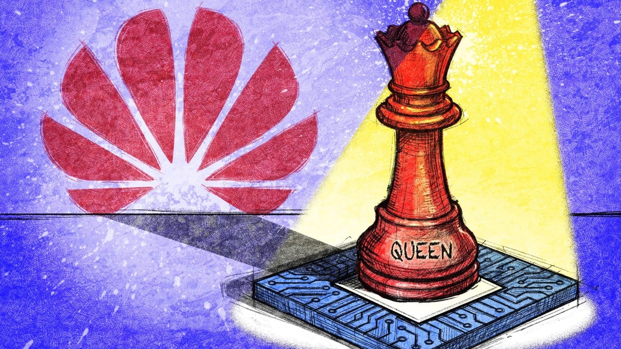
After seven years working in the shadows, He Tingbo stepped back into the limelight last month. The head of Huawei Technologies’ secretive semiconductor business – widely dubbed the company’s “chip queen” – had been out of the public view since 2019, when Washington severed the Chinese company’s global access to advanced technology, including semiconductors. Her retreat into the background became a symbol of Huawei’s battle for survival. That all changed last month on a global academic stage in...
After seven years working in the shadows, He Tingbo stepped back into the limelight last month. The head of Huawei Technologies’ secretive semiconductor business – widely dubbed the company’s “chip queen” – had been out of the public view since 2019, when Washington severed the Chinese company’s global access to advanced technology, including semiconductors. Her retreat into the background became a symbol of Huawei’s battle for survival. That all changed last month on a global academic stage in Shanghai – the IEEE International Symposium on Circuits and Systems. It was there that He introduced the “Tau (τ) Scaling Law”, which Huawei claimed could achieve transistor densities equivalent to the cutting-edge 1.4-nanometre process by 2031 – all without the need for advanced extreme ultraviolet (EUV) lithography machines out of reach due to US sanctions. The announcement ignited a debate across the global semiconductor industry: Had Huawei truly unlocked a revolutionary chapter for China’s drive towards tech self-reliance, or was it just an ambitious theory, or even hype, destined to stumble when it came to the realities of manufacturing? Redefining ‘advanced’ For half a century, the electronics industry treated Moore’s Law – the principle that the number of transistors on a chip doubles roughly every two years – as gospel. But as silicon structures approached atomic limits, geometric scaling was yielding diminishing economic returns and hitting an architectural brick wall. Huawei’s Tau Law is an attempt to break free from this paradigm. It seeks to “redefine what ‘advanced’ means”, using time rather than physical size as the ultimate metric of progress, according to a briefing note issued last week by Shanghai-based semiconductor research firm ICwise. Named after the Greek letter used in physics to denote propagation delay, the law focuses on compressing the time it takes for electronic signals to travel across devices and circuits. Analysts and academics point out that the underlying physics is not entirely new. Instead, Huawei’s breakthrough lies in its ability to bring advanced packaging concepts – usually relegated to back-end manufacturing – into the front-end chip design phase. “Huawei is leveraging design and packaging innovations to achieve some of the benefits typically associated with more advanced process nodes,” said Brady Wang, associate director at Counterpoint Research, adding that techniques like Design-Technology Co-Optimisation have been widely used by global firms for years. However, distilling these disparate academic efforts into a unified law was what made the announcement “historically significant”, said Zhao Chun, a professor in the department of electrical and electronics engineering at Xian Jiaotong-Liverpool University. According to Zhao, the meaning of the framework is directly comparable to Intel co-founder Gordon Moore’s seminal 1965 observation. The physical manifestation of this theory is a proprietary architecture Huawei calls “LogicFolding”. While many industry watchers have dismissed it as a variation of advanced 3D packaging, He Tingbo stressed a crucial distinction: it weaves circuits together with a logic die at a “very small gear ratio” – a measure similar to the relationship between two gears engaged with each other. Traditional 3D stacking or “chiplet” designs simply stitch separate, prefabricated chips closer together. In contrast, LogicFolding redesigns a single chip’s internal blueprint from the ground up, Zhao added. ‘We have the US to thank’ Huawei’s semiconductor ambitions became a matter of national survival after the US blacklisted the company and its chip design unit, HiSilicon, which was later banned from working with global foundries like Taiwan Semiconductor Manufacturing Company (TSMC). After a frantic period of stockpiling advanced chips and components, Huawei’s inventory finally ran dry in 2022, crippling its smartphone business. It was during this crisis that He was tasked with reviving the company’s silicon heart. In a highly emotional internal letter in 2019, He revealed a long-held “spare tyres” strategy drawn up for this exact scenario, comparing the coming push to embarking on the “most tragic and heroic Long March in the history of science and technology”. Recalling those dark days at the IEEE forum last month, He admitted to a period of deep frustration where she felt there was “no way out”. Her epiphany, she said, came from Dujiangyan – the 2,000-year-old irrigation system in China’s southwest Sichuan province, built without modern machinery or electricity. She began to view US sanctions not as an insurmountable wall, but simply as engineering constraints to be solved. That defiance bore fruit with the surprise launch of the Mate 60 Pro smartphone in 2023, powered by the 5G-capable Kirin 9000s processor. A teardown by Canadian research firm TechInsights revealed that China’s top foundry, Semiconductor Manufacturing International Corporation (SMIC), had managed to manufacture the processor with 7nm technology using existing chipmaking tools pushed to their limits. Huawei has since broken its code of secrecy on multiple fronts. Last September, it unveiled a three-year road map for its Ascend AI processors, positioned as domestic alternatives to chips from US giant Nvidia. “There is actually no need to worry about the chip issue,” Huawei’s octogenarian founder and CEO Ren Zhengfei told People’s Daily last year. “By using methods like stacking and clustering, [our] computing performance is comparable to the state-of-the-art level.” Driven by tightening US export controls, Ascend chips are gaining traction in Chinese data centres. Nvidia CEO Jensen Huang recently said that the American titan’s share of China’s high-end AI chip market had plummeted from 95 per cent to virtually zero. The shift has led to a growing sense of confidence in Shenzhen, where Huawei is headquartered. Xu Zhijun, Huawei’s rotating chairman, went as far as to thank Washington for the pressure. “If it weren’t for the US forcing our country, company and industry, we would never have taken on a task like this,” Xu said in an interview with Chinese media following the Tau Scaling Law announcement. “We have the US to thank for enabling our nation’s semiconductor supply chain to truly grow and develop.” A stark choice The strategic implications of the Tau Scaling Law are reverberating globally. While Washington remains fixated on choking off China’s access to advanced lithography hardware over concerns the technology will aid China’s military, Beijing has poured billions into developing home-grown alternatives. In what appears to be a retaliatory move, Beijing has squeezed US tech imports by withholding domestic sales approval for Nvidia’s H200 AI processors – even though Washington had already given the green light for exporting the chips. “Nvidia is likely the most concerned by this development,” said He Hui, director of semiconductor research at Omdia. “Having already lost half of its market share in China, Nvidia now faces a reality where domestic chip performance has nearly closed the gap with the H200.” Responding to the Tau Law announcement, Nvidia’s Huang called the architecture a “breakthrough for Huawei”, though he suggested it posed no immediate threat to the manufacturing hegemony of TSMC – Nvidia’s primary foundry partner. Laila Khawaja, an analyst at Gavekal Research, said she viewed the announcement as a calculated strategic signal from China. Huawei was “presenting foreign governments and companies with a choice: cooperate and share the potential upside from China’s experiment, or risk an alternative Chinese ecosystem that could erode their position in the critical China market – and potentially global markets in the long run,” Khawaja said. The pivotal question remains: Can Huawei truly decouple from EUV lithography? Phelix Lee, a senior equity analyst at Morningstar, notes that LogicFolding effectively bypasses the most advanced chipmaking tools – manufactured by Dutch firm ASML under a functional monopoly – by shifting the engineering burden to reducing data transmission latency. However, Counterpoint’s Wang cautioned that while this approach extends the utility of older deep ultraviolet lithography, or DUV, machines, a significant gap remains in power efficiency, performance, speed and manufacturing throughput when compared to leading-edge EUV-based systems. From theory to reality Translating a theoretical 1.4nm equivalence into commercial reality requires overcoming a mountain of supply chain chokepoints. The most immediate enemy of LogicFolding is heat dissipation. ICwise noted that folding circuits into multiple active layers causes the heat density to jump five to 10 times. Furthermore, the shift of design methodology from 2D to 3D would require dedicated chip design tools, another chokepoint for China. Traditional electronic design automation (EDA) tools are built for 2D flat wiring, while 3D LogicFolding requires multilayer layout, cross-layer timing closure, and cross-layer power integrity analysis – software that the domestic industry is still racing to develop. Major players are rushing to seize the opportunity. Empyrean Technology, one of China’s best hopes in replacing Western EDA tools, said last week that it had developed a set of tools for 3D integrated circuit design as “a key carrier for the landing of Tau scaling law”. Yield is yet another issue. According to ICwise, while Huawei’s 1.5-micrometre bonding pitch is highly advanced, achieving a commercially viable yield rate when stacking three to four active layers remained an extremely difficult task. Because of these hurdles, some experts said Huawei’s playbook cannot be easily copied by others. “We think Huawei’s approach is not replicable, especially in the next five years,” said Morningstar’s Lee. He pointed out that Huawei possessed a rare advantage: a vertically integrated ecosystem that spans chip design, manufacturing partnerships, consumer electronics and network infrastructure all under one corporate roof. Across China’s semiconductor landscape, players from front-end design houses to back-end packaging firms have hailed the framework as a watershed moment for domestic chip self-sufficiency. “[It] is a very advanced design concept,” said Ding Jingfeng, vice-president of technology at Chinese chip packaging giant Tongfu Microelectronics, speaking at an industry forum late last month. “At least in chip design capabilities, Huawei is at the forefront of the world,” he said. “3D design is just beginning, and future designs will be more complex, evolving into more architectures and product forms based on applications.” Han Chaoyang, vice-president of marketing at Hefei-based AI chip company ListenAI – which is currently developing on-device chips for large language model inference – noted that the framework provided vital guidance for domestic firms trying to outmanoeuvre physical fabrication bottlenecks. Han said his company was applying similar system-level co-design principles, enabling 8nm chips to deliver a performance similar to 4nm graphics processing units while deploying optimised large language model algorithms. “It is essentially a declaration, or even an appeal, from Huawei and the semiconductor industry in the post-Moore’s Law era,” Han said. The ultimate proof of concept for Huawei and the broader Chinese tech ecosystem is fast approaching. This autumn, the first commercial iteration of the LogicFolding architecture is expected to debut inside the Kirin processors powering the company’s next generation of smartphones. For the Huawei chip team under He, the “spare tyres” they started building years ago are now keeping Huawei on track. “We not only opened up the road, but also built a highway,” she told People’s Daily after the Tau law was announced.